LAWS OF THERMODYNAMICS:


(i). Zeroth Law of thermodynamics:

If two bodies are in thermal equilibrium and a third body is in thermal equilibrium with any one of the first two bodies, then it can be inferred that all the three bodies are in thermal equilibrium. 

(ii). First Law of Thermodynamics:

        If any system is carried through a cycle then the summation of the work delivered to the surroundings is proportional to the summation of the heat taken from the surroundings.


            ¤         dW  α    ¤                 dQ                    

¤         dW  = J    ¤                 dQ     J is th proportionality constant known as the mechanical
                                    equivalent  of heat = 1 KJ / KNm
           
            ¤         dQ  -    ¤                 dW / J  = 0
            ¤          [                                                                        [dQ  -    dW / J]  = 0


Path:

    If a system passes through a series of state point then it is said to describe a path.

Process:

    Whenever a state change occurs then the system is said to undergo a  process

Cycle:

    If a system starts from a particular thermodyanmic coordinate point, under goes different process and once again comes back to its initial state points it is said to undergo a cycle or thermodyanmic  cycle

Corollary:


(a)  Internal energy is a property.

    Consider a system of two cycles 1 A 2 B 1 and  1 A 2 C 1  

       Applying first law to cycle I: 1 A 2 B 1

1A∫2  [dQ-dW/J] + 2B∫1  [dQ-dW/J]  = 0

1A∫2  [dQ-dW/J] =  - 2B∫1  [dQ-dW/J] 

1A∫2  [dQ-dW/J] =  1B∫2  [dQ-dW] ---- (a)

Applying first law to cycle I: 1 A 2 C1

1A∫2  [dQ-dW/J] + 2C∫1  [dQ-dW/J]  = 0

1A∫2  [dQ-dW/J] =  - 2C∫1  [dQ-dW/J] 

1A∫2  [dQ-dW/J] =  1C∫2  [dQ-dW] ---- (b)

From (a) & (b) we get  1A∫2  [dQ-dW/J] =  1B∫2  [dQ-dW] =   1C∫2  [dQ-dW]

The quantity [dQ-dW/J] is independent of the path.

Any quantity, independent of the path is known as property.

     [dQ-dW/J] is a property.

But we have taken that [dQ-dW/J]= dU and  U is the internal energy for the given mass m. Therefore  internal energy is a property.

(b) Law of conservation of Energy.

    Energy can neither be created not destroyed if mass is conserved.

It is defined as the internal energy remains unchanged if the system is completely isolated.

    if Q=0 ;    W = 0 then  ∆U =0

(c)  Perpetual Motion Machine   of  I kind  ( PMM I) is impossible.

It is imposible to construct an engine which produces work without taking heat from the surrounding.
An engine which can produce work without taking heat from the surrounding is known as PMM I. This is not possible.

ZENER DIODE

  • In  a  general  purpose  PN  diode  the  doping  is  light;  as  a  result  of  this  thebreakdown  voltage  is  high.  If  a  P  and  N  region  are  heavily  doped  then  the breakdown voltage can be reduced.
  • When the doping is heavy even the reverse voltage is low, the electric field atbarrier  will  be  so  strong  thus  the  electrons  in the  covalent  bands  can  break away from the bonds. This effect is known as zener effect.
  • A  diode  which  exhibits  the  zener  effect  is  called  a  zener  diode.  Hence  it  isdefined as a reverse biased heavily doped PN junction diode which operates in breakdown   region.   The   zener   diodes   have   been   designed   to   operate   at voltages ranging from a few volts to several hundred volts.
  • Zener breakdown occurs in junctions which is heavily doped and have narrowdepletion layers. The  breakdown voltage sets up a  very strong  electric field.    This  field  is  strong  enough  to  break  or  rupture  the  covalent  bonds  thereby generating electron hole pairs.
  • Even a small reverse voltage is capable of producing large number of currentcarrier, When a zener diode is operated in the breakdown region care must be taken to see that the power dissipation across the junction is within the power rating  of  the  diode  otherwise  heavy  current  flowing  through  the  diode  may destroy it.
Equivalent Circuit of Zener diode

The schematic symbol and its equivalent circuit are shown in figure 14. It is similar to that of normal diode except the line representing cathode is bent both ends are shown in figure 14.


V-I Characteristics of zenerdiode


The forward characteristic of a zener diode is similar to that of a P N Junction diode. The reverse characteristic of zener diode is obtained as follows.

  • The reverse current that is present at the origin and the knee of the curve isdue to the reverse leakage current due to the minority carriers. This current is specified by stating its value at 80% of the zener voltage Vz
  • As  the  reverse  voltage  is  gradually  increased,  the  breakdown  occurs  at  theknee  and  the  current  increases  rapidly.  To  control  this  current  a  suitable external  resistance  has  to  be  used.  The  maximum  permissible  value  of  the current is denoted by Izmax. The minimum usable current is Izmin
  • The  voltage  across  the  terminals  of  the  diode  for  a  current  Iz  which  is  theapproximate  midpoint  of  the  linear  range  of  the  reverse  characteristics  in called the zener voltage Vz. At the knee point, the breakdown voltage remains constant  between  Izmax  and  Izmin.  This  ability  of  a  diode  is  called  regulating ability and is an important feature of a zenerdiode.

Application of Zener Diode

It can be used


a) As voltage regulators

b) As peak clippers

c) For reshaping waveforms

d) For meter protection against damage from accidental application of excessive voltage

PROGRAMMABLE UNIJUNCTION TRANSISTOR


The programmable unijunction transistor (PUT) is an improved version of UJT.But  PUT  is  a  four  layer  PNPN  device  it  also  known  as  small  version  of thyristors as shown in figure 12.

Its operation is similar to the UJT hence it is always considered with UJT, itstrigger voltage VP can be programmed or decided by the designer via external potential divider [ but in UJT, it is fixed for the given device] thus it is known   as programmable unijunction transistor.

The  symbol  of  PUT  is  shown  in  figure  12.  In  this  case  the  gate  terminal  isconnected to the N region [but in thyristor or SCR gate is connected with P     region], thus the anode and cathode constitute the PN junction which controls the ON and OFF states of PUT.


Usually positive potential is applied to gate with respect to cathode. When theanode voltage is less than gate voltage VG the anode gate junction becomes reverse biased, the PUT is in OFF state.

When the anode voltage exceeds the gate voltage V anode cathode junctionbecomes  forward  biased,  thus  PUT  is  turned  ON.  In  the  ON  state,  the  PUT behaves like other four layer PNPN devices [SCR]. The PUT is also known as complementary SCR [because the gate is connected with ‘N’ layer instead of ‘P’ layer].

Advantages of PUT over UJT


1.  The  switching  voltage  is  easily  yarned  by  changing  Vg  through  the  potential divider.

2. PUT can operate at lower voltages then IC’s. 3. Peak current is lower UJT.

PUT as relaxation oscillator

A PUT can be used as relaxation oscillator it is shown in figure 12. The gate    voltage  VG  is  maintained  from  the  supply  by  the  potential  divider  R1  and  R2  and determines the peak point voltage Vp In the case of the UJT, VP is fixed for a device by  the  dc  supply  voltage.  But  VP  of  a  PUT  can  be  varied  by  varying  the  potential divider it and it Tithe anode voltage VA is less than the gate voltage V the device will remains in its off state.

ZENER DIODE

  • In  a  general  purpose  PN  diode  the  doping  is  light;  as  a  result  of  this  thebreakdown  voltage  is  high.  If  a  P  and  N  region  are  heavily  doped  then  the breakdown voltage can be reduced.
  • When the doping is heavy even the reverse voltage is low, the electric field atbarrier  will  be  so  strong  thus  the  electrons  in the  covalent  bands  can  break away from the bonds. This effect is known as zener effect.
  • A  diode  which  exhibits  the  zener  effect  is  called  a  zener  diode.  Hence  it  isdefined as a reverse biased heavily doped PN junction diode which operates in breakdown   region.   The   zener   diodes   have   been   designed   to   operate   at voltages ranging from a few volts to several hundred volts.
  • Zener breakdown occurs in junctions which is heavily doped and have narrowdepletion layers. The  breakdown voltage sets up a  very strong  electric field.    This  field  is  strong  enough  to  break  or  rupture  the  covalent  bonds  thereby generating electron hole pairs.
  • Even a small reverse voltage is capable of producing large number of currentcarrier, When a zener diode is operated in the breakdown region care must be taken to see that the power dissipation across the junction is within the power rating  of  the  diode  otherwise  heavy  current  flowing  through  the  diode  may destroy it.
Equivalent Circuit of Zener diode

The schematic symbol and its equivalent circuit are shown in figure 14. It is similar to that of normal diode except the line representing cathode is bent both ends are shown in figure 14.


V-I Characteristics of zenerdiode


The forward characteristic of a zener diode is similar to that of a P N Junction diode. The reverse characteristic of zener diode is obtained as follows.

  • The reverse current that is present at the origin and the knee of the curve isdue to the reverse leakage current due to the minority carriers. This current is specified by stating its value at 80% of the zener voltage Vz
  • As  the  reverse  voltage  is  gradually  increased,  the  breakdown  occurs  at  theknee  and  the  current  increases  rapidly.  To  control  this  current  a  suitable external  resistance  has  to  be  used.  The  maximum  permissible  value  of  the current is denoted by Izmax. The minimum usable current is Izmin
  • The  voltage  across  the  terminals  of  the  diode  for  a  current  Iz  which  is  theapproximate  midpoint  of  the  linear  range  of  the  reverse  characteristics  in called the zener voltage Vz. At the knee point, the breakdown voltage remains constant  between  Izmax  and  Izmin.  This  ability  of  a  diode  is  called  regulating ability and is an important feature of a zenerdiode.

Application of Zener Diode

It can be used


a) As voltage regulators

b) As peak clippers

c) For reshaping waveforms

d) For meter protection against damage from accidental application of excessive voltage

SILICON CONTROLLED RECTIFIER


  • It  is  a  four  layered  PNPN  device  and  is  a  prominent  member  of  thyristorfamily.   It consists of   three diodes   connected   back   to   back   with   gate connection or two complementary transistor connected back to back.
  • It  is  widely  used  as  switching  device  in  power  control  applications.  It  canswitch ON for variable length of time and delivers selected amount of power to load.
  • It  can  control  loads,  by  switching  the  current  OFF  and  ON  up  to  manythousand  times  a  second.  Hence  it  possess  advantage  of  RHEOSTAT  and  a switch with none of their disadvantages
Construction

As  shown  in  figure  1  it  is  a  four  layered  three terminal  device, layers  being
alternately  P-type  and  N-type  silicon.  Junctions  are  marked  J1,  J2,  J3  whereas terminals are anode (A), cathode
(C) and gate
(G). The gate terminal is connected to inner P-type layer and it controls the firing or switching of 5CR.

Biasing


The  biasing of  SCR is  shown  in  figure  
1(a).  The  junction  J1  and  J3  become
forward biased while J2 is reverse biased. In figure 1 polarity is reversed. It is seen that now junction J1 and J3 become reverse biased and only J2 is forward biased.

Operation of SCR

  • In  SCR  a  load  is  connected  in  series  with  anode  and  is  kept  at  positivepotential  with  respect  to  cathode  when  the  gate  is  open  i.e.,  no  voltage  is applied at the gate.
  • Under this condition, junctions J1 and J3 are for ward biased and junction J2is reverse biased. Due to this, no current flows through RL and hence the 8CR is cutoff.
  • However when the anode voltage is increased gradually to breakover voltage,then  breakdown  occurs  at  junction  J  due  to  this  charge  carriers  are  able  to flow from cathode to anode easily, hence SCR starts conducting and is said tobe in ON state.
  • The SCR  offers  very  small forward  resistance so that  it  allows infinitely highcurrent.  The  current  flowing  through  the  8CR  is  limited  only  by  the  anode voltage and external resistance.
  • If  the  battery  connections  of  the  applied  voltage  are  reversed  as  shown  infigure 2 the junction J1 and J3 are reverse biased. J2 is forward biased.
  • If  the  applied  reverse voltage is  small  the  SCR is  OFF  and  hence no  currentflows through the device.
  • If the reverse voltage is increased to reverse breakdown voltage, the junctionJ1 and J3 will breakdown due to avalanche effect. This causes current to flow through the SCR.
  • From the above discussion we conclude that the SCR can be used to conduct only in forward direction. Therefore SCR is called as “unidirectional device”.
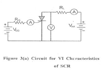
Vl Characteristics of SCR

The  “forward characteristics”   of SCR may be obtained using the figure 3.

The volt-ampere characteristics of a SCR for IG = 0 is shown in figure 3.


  • As the applied anode to cathode voltage is increased above zero, very smallcurrent flows through the device, under this condition the 5CR is off. It will be continued  until;  the  applied  voltage  reaches  the  forward  Breakover  voltage (point A).
  • if  the  anode-cathode  (applied)  voltage  exceeds  the  Breakover  voltage  itconducts heavily the SCR turns ON  and  anode to  cathode voltage decreases quickly  to  a  point  B  because,  under  this  condition  the  5CR  offers  very  low resistance hence it drops very low voltage across it.
  • At this stage the 5CR allows more current to low through it. The amplitude ofthe   current   is   depending   upon   the   supply   voltage   and   load   resistance connected in the circuit.
  • The current corresponding to the point ‘B’ is called the “holding current (IH)”It can be defined as the minimum value of anode current required to keep the     SCR  in  ON  State.  If  the  5CR  falls  below  this  holding  current  the  SCR  turns OFF.
  • If the value of the gate current I is increased above zero, (‘G > O) the SCRturns ON even at lower Breakover voltage as shown in figure 3(b).
  • The region lying between the points OA is called forward blocking region. Inthis  region  5CR  is  OFF’.  The  region  lying  between  the  points  BC  is  called forward conduction region. In this region SCR is ON.
  • Once  the  SCR  is  switched  ON  then  the  gate  looses  all  the  control.  So  SOBcannot  be  turned  OFF  by  varying  the  gate  voltage.  It  is  possible  only  by reducing the applied voltage.
To obtain the “reverse characteristics”the following points are followed.

1.In  this  case  the  SCR  is  reverse  biased,  if  the  applied  reverse  voltage  is increased  above  zero,  hence  a  very  small  current  flows  through  the  SCR.

 Under  this  condition  the  SCR  is  OFF,  it  continues  till  the  applied  reverse voltage reaches breakdown voltage.

2.As the applied reverse voltage is increased above the breakdown voltage, the avalanche  breakdown  occurs  hence  5CR  starts  conducting  in  the  reverse direction. It is shown in curve DE. Suppose the applied voltage is increased to   a very high value, the device may get damaged.

SCR rating

The SCR rating are defined as follows

1)  “Forward  Breakover  voltage”:It   is   the   voltage   at   which   the   5CR  is switched  from  its  OFF  position  to  ON  position.  Its:  values  are maximum  for zero gate current, its values lie in the range of 50 to l200volts

2)  “Holding  current”:  it  is  the  minimum  value  of  anode  current  required  to keep the SCR in ON position.

3)   “Gate  triggering  current”:    It  is  the  value  of  anode  current  necessary  to switch  5CR from  OFF to  ON  position under specified condition. It  is  typically   about 4OmA.

4)   “Average forward current”:   It is the maximum value of anode current at which the 5CR can handle in its ON position. Its value lies in the range of 1 to 1800Amps.

5)   “Reverse breakdown voltage”:   It is the value of reverse voltage between cathode to anode at which the avalanche breakdown occurs.

6)  “Turn ON time – TON”: It can be defined as, the time required to switch it from OFF to ON state when triggering signal is applied. TON decreases if the trigger voltage is increased; TON is increases when anode current increases.

7)   “Turn OFF Time – TOFF”: It is the time required to switch it  from ON to OFF  state  by  dropping  anode  voltage.  TOFF  is  small  if  anode  voltage  in reverse direction and increases with temperature and anode current.

8)  “Gate  Recovery  time”:    It  is  the  time  required  for  which  anode  voltage  is reduced to VH to turn OFF SCR.

Basic Operation of an SCR

The operation of a PNPN device can best be visualized as a specially coupled
pair of transistors as shown in Figure


The  connections  between the  two transistors  are  such that  regenerative  action  can occur when a proper gate signal is applied to the base of the NPN transistor. Normal leakage  current  is  so  low  that  the  combined  hFE  of  the  specially  coupled  two- transistor  feedback  amplifier  is  less  than  unity,  thus  keeping  the  circuit  in  an  off- state  condition.  A  momentary  positive  pulse  applied  to  the  gate  will  bias  the  NPN transistor into conduction  which, in turn,  biases  the  PNP transistor into conduction.    The  effective  hFE  momentarily  becomes  greater  than  unity  so  that  the  specially coupled  transistors  saturate.  Once  saturated,  current  through  the  transistors  is enough to keep the combined hFE greater than unity. The circuit will remain “on” until    it  is  “turned  off”  by  reducing  the  anode-to-cathode  current  (IT)  such  that  the combined  hFE  is  less  than  unity  and  regeneration  ceases;  this  threshold  anode current is the holding current of the SCR.

Electrical Characteristic Curves of Thyristors V-I Characteristics of SCR Device


Methods of Switching on Thyristors There are three general ways to switch thyristors to on-state condition:

  • Application of Gate Signal
  • Static dv/dt Turn-On
  • Voltage Breakover Turn-On
Listed below is a brief description of each method.

Application Of Gate Signal

For an SCR (unilateral device), this signal must be positive with respect to the cathode polarity. A triac (bilateral device) can be turned on with gate signal of either polarity;  however,  different  polarities  have  different  requirements  of  IGT  and  VGT which must be satisfied. Since a diac does not have a gate, this method of turn-on is     not applicable to diacs; in fact, the single major application of diacs is to switch-on   triacs.

Static dv/dt Turn-On

Comes  from  a  fast  rising  voltage  applied  across  the  anode  and  cathode terminals of an SCR or the main terminals of a triac. Due to the nature of thyristor construction,  a  small  junction  capacitor  is  formed  across  each  PN  junction.  Figure 14.14  shows  how  typical  internal  capacitors  are  linked  in  gated  thyristors.  When voltage  is  impressed  suddenly  across  a  PN  junction,  a  charging  current  will  flow which is equal to:

i = C (dv/dt)

When   c   (dv/dt)   becomes   greater   or  equal  to  thyristor  IGT,  the thyristor  switches  on.  Normally,  this  type  of  turn  on  does  not  damage  or  hurt the device providing the surge current is limited. Generally, thyristor application circuits are designed with static dv/dt snubber networks if fast rising voltages are
anticipated.

Voltage Breakover Turn-On

Is the method used to switch on diacs. However, exceeding voltage break over of SCRs and triacs is definitely not recommended as a turn-on method. In the case of   SCRs  and  triacs,  the  leakage  current  increases  until  it  exceeds  the  gate  current required  to  turn-on  these  gated  thyristors  in  a  small  localized  point.  When  turn-on occurs by this method, there is localized heating in a small area which may melt the    silicon  or  damage  the  device  if  di/dt  of  the  increasing  current  is  not  sufficiently limited.  Diacs  used  in  typical  phase  control  circuits  are  basically  protected  against excessive  current  at  breakover  as  long  as  the  firing  capacitor  is  not  excessively large. When diacs are used in a zener function, current limiting is necessary.

COMMON COLLECTOR CONFIGURATION OF A TRANSISTOR


COMMON COLLECTOR CONNECTION

In  this  configuration  the  input  is  applied  between the  base  and  the  collector and  the  output  is  taken  from  the  collector  and  the  emitter.  Here  the  collector  is common to both the input and the output circuits as shown in Fig.

                                                       Common Collector Transistor Circuit

In  common  collector  configuration  the  input  current  is  the  base current  IB  and  the output current is the emitter current IE. The ratio of change in emitter current to the  change in the base current is called current amplification factor.

It is represented by 


COMMON COLLECTOR CIRCUIT

A test  circuit  for determining the  static characteristic  of an NPN transistor is shown in Fig. In this circuit the collector is common to both the input and the output circuits.   To   measure   the   base   and   the   emitter   currents,   milli   ammeters   are connected in series with the base and the emitter circuits. Voltmeters are connected   across the input and the output circuits to measure VCE and VCB

INPUT CHARACTERISTICS

                                                Common Collector Input Characteristic Curve


  • It  is  a  curve  which  shows the  relationship  between the  base  current,  IB and the collector base voltage VCB at constant VCE This method of determining the characteristic is as follows.

  • First, a suitable voltage is applied between the emitter and the collector. Nextthe  input  voltage  VCB  is  increased  in  a  number  of  steps  and  corresponding values of IE are noted.

  • The base current is taken on the y-axis, and the input voltage is taken on the x-axis. Fig. shows the family of the input characteristic at different collector- emitter voltages.

  • The following points may be noted from the family of characteristic curves.  1.Its  characteristic  is  quite  different  from  those  of  common  base  andcommon emitter circuits.
2.When VCB increases, IB is decreased.

Output Characteristics

  • It is a curve which shows the relationship between the emitter current l and collector-emitter voltage, the method of determining the output characteristic is as follows.

  • First,  by  adjusting  the  input  a  suitable  current  IB  is  maintained.  Next  VCB increased in a number of steps from zero and corresponding values of IE are  noted.

  • The above whole procedure is repeated for different values of IB. The emitter current  is  taken  on  the  Y-axis  and  the  collector-emitter  voltage is  taken  on the X-axis.

  • Fig shows the family of output characteristics at different base current values. The following points are noted from the family of characteristic curves.
                                         Common Collector Output Characteristic Curves

1.This  characteristic  is  practically  identical  to  that   of  the  common  emitter circuit.

2.Its current gain characteristic for different values of VCE is also similar to that of a common emitter circuit.

Swinburne’s Test Method For Testing DC shunt motor


For a d.c shunt motor change of speed from no load to full load is quite small. Therefore, mechanical loss can be assumed to remain same from no load to full load. Also if field current is held constant during loading, the core loss too can be assumed to remain same.


      In this test, the motor is run at rated speed under no load condition at rated voltage. The current drawn from the supply IL0 and the field current If are recorded (figure 40.4).


     Since the motor is operating under no load condition, net mechanical output power is zero.
Hence the gross power developed by the armature must supply the core loss and friction &
windage losses of the motor. Therefore,

                                        Pcore + Pfriction = (V − I a 0 ra ) I a 0 = Eb 0 I a 0


       Since, both Pcore and Pfriction for a shunt motor remains practically constant from no load to
full load, the sum of these losses is called constant rotational loss i.e.,

                                 constant rotational loss, Prot = Pcore + Pfriction

In the Swinburne's test, the constant rotational loss comprising of core and friction loss is
estimated from the above equation.


After knowing the value of Prot from the Swinburne's test, we can fairly estimate the
efficiency of the motor at any loading condition. Let the motor be loaded such that new current
drawn from the supply is IL and the new armature current is Ia as shown in figure 40.4. To
estimate the efficiency of the loaded motor we proceed as follows:

Input power to the motor, Pin=VIL

Cu loss in the field circuit Pfl=VIf

Power input to the armature=vIa

Cu loss in the armature circuit=Ia2 Ra


Net mechanical output power, Pnet mech=Eb Ia- Prot


The estimated value of Prot obtained from Swinburne’s test can also be used to estimate the

efficiency of the shunt machine operating as a generator. In figure 40.5 is shown to deliver a

load current IL to a load resistor RL. In this case output power being known, it is easier to add

the losses to estimate the input mechanical power.


Efficiency of the generator, η= Pin,mech/VIl


The biggest advantage of Swinburne's test is that the shunt machine is to be run as motor
under no load condition requiring little power to be drawn from the supply; based on the no load
reading, efficiency can be predicted for any load current. However, this test is not sufficient if we
want to know more about its performance (effect of armature reaction, temperature rise,
commutation etc.) when it is actually loaded. Obviously the solution is to load the machine by
connecting mechanical load directly on the shaft for motor or by connecting loading rheostat
across the terminals for generator operation. This although sounds simple but difficult to
implement in the laboratory for high rating machines (say above 20 kW), Thus the laboratory
must have proper supply to deliver such a large power corresponding to the rating of the
machine. Secondly, one should have loads to absorb this power.


LPT PRINTER PARALLEL PORT part-1


1. PREFACE
 
Every PC has one or more LPT printer parallel port adapter. This adapter have several I/O port. In old PC, the parallel port may be set at video adapter card or at separate I/O device card (multi I/O). In the beginning, this port only used for printer device, so the data port (8 bits) only used for sending data to the printer and can not receive data from the outside. Now, everything has changed. Many device were connected to this parallel port, so the design always change time to time, even the characteristic always the same (i.e. new card usually used a new chip design and have more capabilities, like bidirectional data transfer, can be configured to work more faster, etc., etc.). Ok, lets we explore more about it now.

2. SIGNAL NAME & PURPOSE
 
Because the parallel port have many location, so the port also follow this procedure and always standard. For our description, DP refer to printer Data Port, PC refer to Printer Control and PS refer to Printer Status. Tabel-1 shown each port and their function.


LPT 0 LPT 1  LPT 2  Operation  Description
3BC Hex  378 Hex  278 Hex  (Read)/Write  Data Port (DP), 8 bits 
3BD Hex  379 Hex  279 Hex  Read only  Printer Status (PS), 5(6) bits 
3BE Hex  37A Hex  27A Hex  Read/Write  Printer Control (PC), 4(6) bits 
Tabel-1. LPT location, function and description.

a. Data Port (DP)
 
DP has 8 bits length. It means that it can be transfer or sending data 8 bits long at a moment time. The old PC has LPT parallel port function only for sending data. Many devices nowadays have attached to this port and can work bidirectional. For examples : scanner device, many storage device like zip drive, etc., etc. This means that this port can be used for sending or receiving data. New card can be configured to work like this (eg:bi-directional port), but old one don't. In the end of this article, you can change the ability of the old card, so that it can be used to receive data. Data bits are naming as DP-0 trought DP-7. For the relation number to the D-25 socket refer to the LPT Connector. DP port can sink 24 mA at logic 0 and can source 2.6 mA at logic 1. Notice that the external device don't try to pull these DP lines to ground for a long period. The latch IC could be burn.

b. Printer Control (PC)
 
PC is used for controlling the function of printer. Only 4 bits used by printer and 1 bit used for interrupt enable flag. The complete description was shown on Figure-1. The interrupt enable bit flag used for handshake operation between computer and printer, so that the device can work with a little time of CPU to interfere. The most important things must be taken if you connect your own device are : the PC-0, PC-1 and PC-3 logic are inverting at socket connector terminal. This means that, when you send logic 1 (high) to this related bit, the logic output terminal is 0 (low). The PC-2 and PC-4 are normal. The PC-5 to PC-7 are not used by the hardware circuit. Note that, PC-4 bit only for the adapter card function. This means this bit does not connect out to the connector terminal. PC port can sink 7 mA at logic 0 and can source 0.6 mA at logic 1. Besides that, in some PC/AT's LPT adapter card, bit PC-5 is used for control direction (and also in bi-directional card). It means that, if this bit is high, DP port can act as input port, the latch output is tri-state. Data from outside can be read from DP port.


c. Printer Status (PS)
 
PS port used for feedback signal from printer to the computer. Only 5 MSB bits are used, the 3 LSB bits not used. The complete description was shown on Figure-2. Only 1 bit is inverting input ie. PS-7 use for busy signal. PS-6 bit use for acknowledge signal This signal used when the printing goes on with interrupt handshake operation. This is a hardware interrupt. In some PC/AT's card and bi-directional card, PS-2 is used to reflex the state of IRQ, weather it is on or off state. This bit only for internal use.


3. CONNECTOR TERMINAL
 
LPT port adapter use a female DB-25 D-shell connector type. The complete connection can be seen in Figure-3. Only 17 terminals be used, and the rest are grounded all. This is a standard terminal connection. The connection are the same for all of the LPT's connector. Figure-4. show the connection between printer to the LPT adapter.


4. PRINTER INTERFACE DESCRIPTION
 
LPT printer parallel interface in PC computer type have specification like this :
  • Data transfer rate : 1000 cps (maximum)
  • Synchronization : by externally-supplied STROBE pulses.
  • Handshaking -ACK or +BUSY signals.
  • Logic level : input data and all interface control signal are compatible with the TTL level.
Generally this specification allways the same for new card design, but the data transfer may vary between one design and another. This type of interface also called CENTRONICS interface and have the data transfer sequence time as shown in Figure-5.


STROBE pulse to read data in. Pulse width must be more than 0.5 us at receiving terminal. The signal level normally high. Read in of data is performed at the low level of this signal. ACK signal is approximately 5 us pulse. Logic low indicates that data has been received and the printer is ready to accept other data. BUSY signal high indicates that the printer can not receive data. This signal becomes high in the following cases :
    • During data entry
    • During printing operation
    • In offline state
    • During printer error status
    Note that : centronics interface only valid for printer timing sequence, and not for other device which used LPT printer adapter.

PC PROTOTYPE CARD part-3


G. DECODING

 
Build a prototype card implies how to decode the addresses. There are 2 types of decoding techniques, i.e.: I/O decoding and Memory decoding. If the hardware used I/O map for its port, it was called I/O mapped I/O, and if the hardware used memory map for its port, it was called memory mapped I/O.
What are the different point between this 2 types of decoding ?
If we use I/O mapped I/O port, we only can access this port by using the IN and OUT commands. If we used memory mapped I/O port, we can access this port by using all of the commands usually used for data transfer like MOVE, STORE, or any other modes of addressing transfer. In the I/O mapped I/O port, we can only used the reserved location among 1024 locations which implemented for. In the memory mapped I/O, we can used the upper location of memory above A0000 hex, and it is more wisely if we use the upper limit of FXXXX hex boundary which is still available; e.g.: start at F0000 hex, because many of the available locations can be used for UMB block or for XMS pages. 


  •  I/O Mapped I/O Decoding
     
    Because of the I/O restriction, we only use 10 address lines (A0 ~ A9). Besides that we need AEN line, -IOR & -IOW, -I/O CH RDY (for some card that needs wait states). Notes that, adding wait states will make the computer to run more slowly. It is more wisely not to use this line.How we decoding this lines ? For example; we use address location 300 hex which is still available for prototype card. We need 8 consecutive I/O port locations. The decoding is as follows :
    AEN A9 A8      A7 A6 A5 A4      A3 A2 A1 A0
     0  1  1     0  0  0  0    1 X  X  X   =  300 ~ 307 hex
    So the decode is :
    ___    _ _ _ _
    AEN A9A8A7A6A5A4A3A2A1A0
     
     
  • Memory Mapped I/O Decoding
  •  
    Because of DOS restriction, we only use 20 address lines (A0 ~ A19). Besides that we need -MEMR & -MEMW lines.For example; we used 16 consecutive I/O start at the F0000 hex location. So the decoding is as follows :   A19 A18 A17 A16  A15 A14 A13 A12  A11 A10 A9 A8  A7 A6 A5 A4  A3 A2 A1 A0
     1  1   1  1    0  0   0  0    0  0  0  0   0  0 0  0   X  X X  X
    = F0000 ~ F000F hex
    So the decode is :
                  _  _   _  _  _   _  _  _ _ _  _ _
    A19A18A17A16A15A14A13A12A11A10A9A8A7A6A5A4A3A2A1A0
     
     
H. EXPANDING I/O MAP

 
What are you doing if you run out all of the I/O location ?
There are still more techniques to take advantage of this problem. One is to utilise the upper address line (A10 to A15). On the faceof it this is unacceptable, since these address lines are not decoded by either the system hardware or any expansion cards. These items of hardware will therefore respond to "echoes" of their base addresses, making addresses above 3FFH unuseable. However this problem is avoided if we only use addresses that are "echoes" of the still available address range in the upper block of 512 addresses. For example if the range in 300H to 31FH (32 consecutive I/O ports) are still available, we can expanded it to the limit of 16 x 32 consecutive I/O ports by implemented the above technique. By decoding one or more of the upper address lines as well as the lower 10 address lines, these 32 addresses can effectively be used over and over again, with one set of hardware using the base address range, and each additional piece of hardware using a different "echo" address range. This gives what should be more than enough input/output addresses to satisfy even the most prolific expansion card builder.
The second technique is by used an I/O port as an indexed port like used by video display adapter port. This technique let us to expand 8 I/O ports by used only 2 of the existing I/O port addresses, i.e.: one for the indexed port and the other for the enable port.


PC PROTOTYPE CARD part-2

C. I/O MAP


IBM PC computer mapped its I/O by used address decoder. There are 400 Hex I/O address locations preserved. Some have been used for its own purpose and some used by the external cards and some are still not been use yet. Tabel A-1. show some of these I/O address used for. In fact, I/O address locations can be as much as 220 locations. But in the previous design it is not used all the address lines. Only 10 lines were used, i.e.: 210 = 1024 locations (400 Hex). If you run out these locations all, there is still way to get some of the locations by used the decoder techniques or by used indexed I/O map. This will be describe later.

SanDisk 6-in-1 PC Card Adapter ( SDAD-67-A10, Retail Package)Transcend - Card adapter ( CF I ) - PC Card 
 

ADDRESS DEVICE

S


Y


S


T


E


M


B


O


A


R


D


 I


/


O


000H ~ 01FH DMA Controller 1, 8237A-5
020H ~ 03FH Interrupt Controller 1, 8259A, Master
040H ~ 05FH Timer, 8254-2
060H ~ 06FH Keyboard Controller, 8254
070H ~ 07FH Real Time Clock, NMI (Non Maskable Interrupt) Mask
080H ~ 09FH DMA (Direct Memory access) page register, 74LS612
0A0H ~ 0BFH Interrupt Controller 2, 8259A
0C0H ~ 0DFH DMA Controller 2, 8237A-5
0F0H Clear Math Co-Processor busy
0F1H Reset Math Co-Processor
0F8H ~ 0FFH Math Co-Processor
1F0H ~ 1F8H Fixed Disk Controller

E


X


P


A


N


S


I


O


N


C


H


A


N


N


E


L


I


/


O


200H ~ 207H Game I/O Controller
210H ~ 217H Expansion Slot
220H ~ 24FH Reserved
278H ~ 27FH Parallel Printer Port 3 (LPT-3)
2E8H ~ 2EFH Serial Port 4 (COM-4)
2F0H ~ 2F7H Reserved
2F8H ~ 2FFH Serial Port 2 (COM-2)
300H ~ 31FH Prototype Card
320H ~ 32FH Fixed Disk Controller
360H ~ 36FH Reserved
378H ~ 37FH Parallel Printer Port 2 (LPT-2)
380H ~ 38FH SDLC, Bisynchronous 2
3A0H ~ 3AFH Bisynchronous 1
3B0H ~ 3BBH Monochrome Display Adapter
3BCH ~ 3BFH Parallel Printer Port 1 (LPT-1)
3C0H ~ 3CFH EGA/VGA Adapter Controller
3D0H ~ 3DFH Color/Graphics Monitor Adapter (CGA Adapter)
3E8H ~ 3EFH Serial Port 3 (COM-3)
3F0H ~ 3F7H Floppy Disk (Diskette) Controller
3F8H ~ 3FFH Serial Port 1 (COM-1)
Tabel A-1. I/O map for AT computer.
As we can see from the tabel, I/O port in the PC divided in 2 section, i.e.: direct addressing mode (0 ~ FFH port) are used for system I/O purpose, and indirect mode used by another peripheral which connected to the I/O slots.

Transcend 4 GB 133x CompactFlash Memory Card TS4GCF133High Speed 11Mbps PCMCIA 21 in 1 Card Adapter Reader, support SDHC up to 32GB 

The first decision that has to be made when designing a PC prototype card is just where in the input/output map it should be placed. As explained previously, only 1024 of the 65536 possible places for input/output addresses are availabel on a PC, and the lower 512 addresses are reserved for the computer's internal hardware. Much of the upper block of 512 addresses are reserved for essential and standard expansion cards such as serial ports, and display adapters. We can only use the upper block of 512 addresses for our add-ons cards. There are still more places as mark by reserved that are not been used yet by any cards. We can use it. Even the prototype card has the location itself, it can't make a guarantee that these location are still reserved for our purpose, because many company had built their own card that used this location (include one that introduce by the IBM). Besides the standard card, there are many cards was introduced in the market this day, like video card (VCD or DVD card), TV card, radio card, etc ... etc. This also have several I/O locations that can be choose when installed in the first time. Be sure to check your configuration of I/O ports.

D. MEMORY MAP
 
In the first PC design of memory architecture, memories implemented to it's limit 1 MB boundary (220 as the address only 20 address lines). But not all of this location filled with memories. 216 location (640 kB) was fillled by RAM (Random Access Memory) for the system, program and temporary data. The upper portion was filled with ROM (Read Only Memory) by parts, depends of the configuration of the system; system initialization program, POST (Power On Self Test), BIOS (Basic Input/Output System), BASIC system, display controller, hard disk controller, etc ... etc. This upper portion location also called the UMB (Upper Memory Block) area. If we used DOS version 4.00 and up, we can activated this UMB area to store some portion of the system by put the 'DOS=UMB' statement in the CONFIG.SYS file. But the EMM386.EXE file must be installed first. This ability also valid for any other program if we use the 'LOADHIGH= . . .' statement.
Then the PC design architecture was developing the ability to expanded memory. This technique was development by Lotus-Intel-Microsoft, so become the standard EMS (Expanded Memory Specification) and also called LIM-EMS standard. The alocation method used UMB to map the expanded memory. 16 kB each block and called memory page. Up to 4 pages can be accesses at a time. We can used this option (or any programs which used this standard) by installed EMM386.EXE in the CONFIG.SYS file.
When the AT architecture was introduced, the limit of memory to implemented becomes more wide; 80286 CPU could be implemented up to 16 MB location (24 address lines) and 80386 CPU up to 4 GB (32 address lines). But because of the old design of DOS system, only 1 MB (20 address lines) can be accesses by DOS (DOS run in real mode). To accesses the upper 1 MB, DOS must run in protected mode. These upper 1 MB memory are called XMS (Extended Memory Specification) and can be accesses if we installed EMM386.EXE in the CONFIG.SYS  file too, or in the new system like windows system, it was used a DOS Extender program; DPMI, VCPM, etc ... etc. The first 64 kB memory location upper 1 MB memory also called HMA (High Memory Area). This location only for store the data not to execute the program. DOS also kept its data in it by the 'DOS=HI' statement. But the 'HIMEM.SYS' file must be installed first in the CONFIG.SYS file.
Fig. D-1. shows the memory map for the AT computer system. Its also included, memory location used by any programs and drivers, so we could see the whole system by hardware and software.
Fig. D-1. Memory Map of PC/XT/AT computer system.  
E. HARDWARE INTERRUPT
  
In the earlier PC design, only 1 PIC (Programmable Interrupt Controller) implemented, and in the new design, it was added 1 more (cascade). These hardware interrupts have the priority level. Tabel. E-1. shows the complete hardware interrupts and their priority level in PC system design.

PPA 1134 PCMCIA to Compact Flash Adapter - Card adapter ( CF I ) - CardBusEye-Fi Pro X2 8 GB Class 6 SDHC Wireless Flash Memory Card EYE-FI-8PC 


Hardware Int. No.


Desc. Master PIC


Desc. Slave PIC


Interrupt Vector Table No.


M


A


S


T


E


R


P


I


C


IRQ 0 Timer Int. (8253 PIT channel 0)
  
INT 08H
IRQ 1 Keyboard Int. INT 09H
IRQ 2 Reserved (cascade), Clock Int. Slave PIC (see below) INT 0AH
IRQ 3 Serial Port 2 (COM-2)
   
INT 0BH
IRQ 4 Serial Port 1 (COM-1) INT 0CH
IRQ 5 Fixed Disk Controller Int. INT 0DH
IRQ 6 Floppy Disk Controller Int. INT 0EH
IRQ 7 Parallel Printer Port Int. INT 0FH
IRQ 8
   
Real Time Clock INT 70H

S


L


A


V


E


P


I


C


IRQ 9 Software Redirect to IRQ2 INT 71H
IRQ 10 Reserved INT 72H
IRQ 11 Reserved INT 73H
IRQ 12 Reserved INT 74H
IRQ 13 Coprocessor INT 75H
IRQ 14 Fixed Disk Controller INT 76H
IRQ 15 Reserved INT 77H
Tabel. E-1. Hardware Interrupts Vector Tabel for AT Computer.

F. INTERRUPT VECTOR TABLE (IVT)
 
IVT is a table locate at 00000 hex. This table has 400 hex length. This table implemented on the Intel design architecture. In the begining, this location is to be used for the processor purpose, but in the PC design architecture the purpose is expanded. It's consist of a pair of pointer location; i.e.: CS:IP; where CS for code Segment and IP for Index Pointer. The size is 16 bit each. This pair of location consist of the routine program to do some task. The related function in the program is, location 00000 ~ 00003 hex used for INT 0, location 00004 ~ 00007 hex used for INT 1, and so on. The task for each interrupt is listed in Tabel. F-1. This table also a combined between hardware interrupt and software interrupt. We can also modified this interrupt to do some task for our purpose just by changing the interrupt pointer location not the whole routine.


INT. NO.

DESCRIPTION

INT. NO.

DESCRIPTION

INT 00 H

Division by Zero

INT 01 H

Single Stepping

INT 02 H

Non Maskable Interrupt

INT 03 H

Break Point

INT 04 H

Overflow (INTO)

INT 05 H

Print Screen

INT 06 H

Reserved

INT 07 H

Reserved

INT 08 H

Clock Tick (Hardware)

INT 09 H

Keyboard (Hardware)

INT 0A H

Reserved (Cascade PIC)

INT 0B H

COM-2 (Hardware)

INT 0C H

COM-1 (Hardware)

INT 0D H

Fixed Disk (Hardware)

INT 0E H

Floppy Disk  (Hardware)

INT 0F H

LPT (Hardware)

INT 10 H

Video (Display)

INT 11 H

Device List

INT 12 H

Memory Size (for PC/XT system)

INT 13 H

Disk Drive (Software)

INT 14 H

COM (Software)

INT 15 H

Cassette (for PC/XT system)

INT 16 H

Keyboard Input (Software)

INT 17 H

LPT (Software)

INT 18 H

ROM BASIC (for PC/XT system)

INT 19 H

Bootstrap Startup

INT 1 H

Time of Day (TOD)

INT 1B H

Control Break

INT 1C H

Timer Tick

INT 1D H

Video Parameter Table

INT 1E H

Disk Drive Parameter Table

INT 1F H

CGA Video Graphic Character Table

INT 20 H

Program Terminate

INT 21 H

Various DOS Function

INT 22 H

End Routine Pointer

INT 23 H

DOS Control - C

INT 24 H

Critical DOS Error

INT 25 H

DOS Absolute Disk Read

INT 26 H

DOS Absolute Disk Write

INT 27 H

Terminate and Stay Resident

INT 28 H

Reserved

INT 29 H

Reserved

INT 2A H

Reserved

INT 2B H

Reserved

INT 2C H

Reserved

INT 2D H

Reserved

INT 2E H

Reserved

INT 2F H

DOS Multiplex Function
INT 30 H ~ INT 3F H Reserved

INT 41 H

Reserved

INT 41 H

Fixed Disk Parameter Table

INT 42 H

Reserved

INT 43 H

EGA/VGA Video Graphic Character Table

INT 44 H ~ INT 5F H

Reserved

INT 60 H ~ INT 66 H

User

INT 67 H

LIM EMS Manager

INT 68 H ~ INT 7F H

Reserved (some used by slave PIC)

INT 80 H ~ INT 85 H

BASIC

INT 86 H ~ INT F0 H

BASIC Interpreter

INT F1 H ~ FF H

Reserved
Tabel F-1. Interrupt Vector Table for PC/XT/AT Computer.


Followers