The phenomenon of increasing in electrical conductivity of the crystal with respect to the incident light radiation onto the crystal is called photoconductivity.
Principle:
When photons of energy equal to is incident on the crystal, then the crystal absorbs the energy and creates an electron hole pair, (ie) electrons from valence band goes to conduction band, thereby creating a hole in valence band. In this case both electrons and holes will contribute electrical conductivity and these detectors are called photoconductive detector.
Photoconductive Gain:

An important advantage of the photoconductive detector is the gain of the device (ie) it can produce more number of electron hole pairs for a single incident photon on it.
Let us consider a Photoconducting material in the form of slab of length ’L’ and area ‘A’ biased with the help of external circuit. The load resistance RL is used to control the sensitivity and the blocking capacitor ‘C’ is used to remove the dc component when light is falling on the detector.
In the absence of light signal:
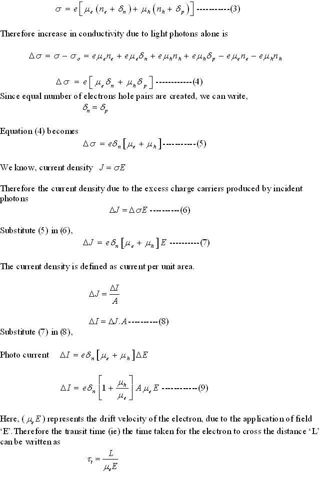
In the absence of a light signal, the current will flow through the circuit due to bias voltage. Let ne and nh be the electron and hole densities without light respectively, then

In the presence of light signal:
Now when the light is allowed to fall on the detector, electron hole pairs are generated equally. These excess carriers increase the conductivity. If and are the excess carrier densities of electrons and holes respectively, then the electrical conductivity due to addition of these charge carriers is

No comments:
Post a Comment