DIODE SWITCHING TIMES


To understand the various switching times, consider simple diode circuit and an input waveform as shown in the Fig.

                                                           Simple diode circuit      

                                              
The following events will take place due to the nature of the applied voltage  

Event  1:  Till  time t the forward voltage  applied  is VF  and  diode  is  forward  biased. The value of R is  large enough such that drop across forward biased diode is very     small  compared to  drop across  R. The forward current  is then
neglecting
forward resistance of diode.


Event 2: At time t the applied voltage is suddenly reversed and reverse voltage of -
VR  is  applied  to  the  circuit.  Ideally  diode  also  must  become  OFF  from  ON  state instantly. But this does not happen instantly.


The number of minority carriers take time to reduce from p no to zero at the junction Due to this, at t1 current just reverses and remains at that reversed value IR till the minority carrier concentration reduces to zero. This current is given by -IR = -VR / R. This continues to flow till time t


Event3: From t onwards, the diode voltage starts to reverse and the diode current
starts  decreasing  as  shown  in  the  Fig.  At  t  =  t;  the  diode  state  completely  gets reversed and attains steady state in reverse biased condition.

The total time required by the diode which is the sum of storage time and transition     time, to recover completely from the change of state is called reverse recovery time
of  the  diode  and  denoted  as  trr.  This  is  an  important  consideration  in  high  speed switching applications.


The reverse recovery time depends on the RC time constant where C is a transition capacitance of a diode. Thus the transition capacitance plays an important role in the switching  circuits  using  diodes.The  total  switching  time  trr  puts  the  limit  on  the maximum  operating  frequency  of  the  diode.  Hence  trr  is  an  important  datasheet specification.  To  minimize  the  effect  of the reverse  current,  the  time  period  of  the operating frequency must be at least ten times trr.


where fmax is the maximum operating frequency.

REVERSE BIASED DIODE


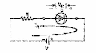
The Fig shows the reverse bias diode. The reverse voltage across the diode VR    while  the  current  flowing  is  reverse  current  ‘R  flowing  due  to  minority  char carriers. The graph of ‘R against VR is called reverse characteristics of a diode.

As reverse voltage is an increased, reverse current increase initially but after
a  certain  voltage,  the  current  remains  constant  equal  to  reverse  saturation current 10 though reverse voltage is increased.


The point A where breakdown occurs and reverse current increase rapidly is called knee of the reverse characteristics.


FORWARD RESISTANCE OF A DIODE


The resistance offered by the p-n junction diode in forward biased condition is called forward resistance. The forward resistance is defined in two ways

1) Static Forward Resistance

This is the forward resistance of p-n junction diode when p-n junction is used in d.c. circuit and the applied forward voltage is d.c. This resistance is denoted as RF and is calculated at a particular point on the forward characteristics.

Thus at a point E shown in the forward characteristics, the static resistance RF is defined as the ratio of the d.c. voltage applied across the p-n junction to the d.c. current flowing through the p-n junction.
RF = Forward d.c. voltage/Forward d.c. current  RF =OA/OC    at point E


2) Dynamic forward resistance


The resistance offered by the p-n junction under a.c. conditions is called dynamic resistance denoted as rf.
Consider the change in applied voltage from point A to B shown in the Fig. 1.18. This  s denoted as AV. The corresponding change in the forward current is from point C to D. I is denoted as J. Thus the slope of the characteristics is t\l/AV. The reciprocal of the e is dynamic resistance rf.

rf = V/ I

=1/slope of forward characteristics


COMPLETE V-I CHARACTERISTICS OF A DIODE


 The complete V-I characteristics of a diode is the combination of its forward as well as reverse characteristics.

In forward characteristics, it is seen that initially forward current is small as long as the bias voltage is less than the barrier potential.


At  a certain  voltage close to  barrier  potential, current increases rapidly.  The voltage  at  which  diode  current  starts  increasing  rapidly  is  called  as  cut  in voltage. It is denoted by V

Below this voltage, current is less than 1% of maximum rated value of diode current. The cut-in voltage for germanium is about 0.2V while for silicon it is 0.6 V.

The  voltage  at  which  breakdown occurs  is  called  reverse  breakdown  voltage denoted as VBR


REVERSE BIASED DIODE


The Fig shows the reverse bias diode. The reverse voltage across the diode VR    while  the  current  flowing  is  reverse  current  ‘R  flowing  due  to  minority  char carriers. The graph of ‘R against VR is called reverse characteristics of a diode.

As reverse voltage is an increased, reverse current increase initially but after
a  certain  voltage,  the  current  remains  constant  equal  to  reverse  saturation current 10 though reverse voltage is increased.


The point A where breakdown occurs and reverse current increase rapidly is called knee of the reverse characteristics.


Elastomers: (Rubber)


     Rubbers are high polymers, which have elastic properties in excess of 300 percent. Thus, a rubber-band can be stretched to 4 to 10 times its original length and as soon as the stretching force is released, it returns to its original length, the coiled Elastomers chain of natural rubber (Poly isoprene).


Bio-Materials:


“Bio-materials are defined as synthetic materials that can be implanted in the body to provide special prosthetic functions or used in diagnostic, surgical and therapeutic applications without causing adverse effect on blood and other tissues”

    Bio-materials have been developed from among metals, ceramics and polymers.

Metallic Bio-materials:


    Metals are used as bio-materials due to their excellent electrical and thermal conductivity and mechanical properties. Since some electrons are independent in metal, they can quickly transfer an electric charge and thermal energy. The mobile free electrons act as the binding force to hold the positive metal ions together, this attraction is strong, as evidenced by the closely packed atomic arrangement resulting in high specify gravity and high melting points of most metals.

    Since the metallic bond is essentially non-directional, the positions of the metal ions can be altered without destroying the crystal structure resulting in a plastically deformable solid.

Uses:

    Some metals are used as passive substitutes for hard tissue replacement such as total hip and knee joints, for fracture healing aids as bone plates and screws, spinal fixations devices, and dental implants because of their excellent mechanical properties and corrosion resistance. Some metallic alloys are used for more active roles in devices such as vascular stents, catheter guide wires, orthodontic arch wires and cochlea implants.

Ceramic Bio-materials:


    Ceramic which are used as bio-materials are classified as bioceramics, the relative inertness to the body fluids, high compressive strength, and aesthetically pleasing appearance led to the use of ceramics in density as dental crown. Some carbons have found use as implants especially for blood interfacing applications such as heart valves.

    Due to high specific strength as fibers and their biocompatibility, ceramics are also being uses as reinforcing components of composite implant materials and for tensile loading applications such as artificial tendon and ligaments.

Medical applications of polymeric biomaterials:

Polyvinyl chloride:

    Blood and solution bag, surgical packaging, IV sets, dialysis devices, catheter bottles, connectors, and cannulae.

Polyethylene:

    Pharmaceutical bottle, nonwoven fabric, catheter, pouch, flexible container, and orthopaedic implants.

Poly propylene:

    Disposable syringes and reservoirs, membrane for blood dialyzer, implantable ocular lens and bone cement.

Polysterene:

    Tissue culture flasks, roller bottles, and filter waves.

Polyethylenter phthalate:


        Implantable suture, mesh, artificial vascular grafts and heat valve.

Polytetra fluoroethylene:

    Catheter and artificial vascular grafts.

Polyurethane:

    Packaging film, catheters, sutures and mould parts.

Non-Linear Materials:


We know that a light wave is electro magnetic in nature. When it propagates through a material, it changes the properties of the medium, such as the refractive index. It depends on the electric and magnetic fields associated with the light beam. For example the non-linear properties of the material will be absent if the incident light beam is of low intensity, since the electricfields associated with the light beam is very weak. On the other hand, for a high intensity light beam such as laser, the non-linear effect will be more strong and interesting.

Classifications:  


    The materials which are used to produce the non-linear optical effects are classified into two categories, namely, passive and active.

Passive materials:


    The materials which are simply used as catalyst without imposing their characteristic internal resonance frequencies on to the incident beam of light are known as passive materials and the effect is known as passive optical effect.


Active materials:


    The materials which impose their characteristic resonance frequencies onto an incident beam of light are known as active materials. The corresponding effect known as active non-linear effect.

Properties:


Polarization:

    When a light beam is incident on a non-linear materials. The electric field interacts with an atom in the material. As a result, electric dipoles are created and hence, an induced charge polarization is produced in the material.
    The magnitude of the polarization depends on the applied electric field(E), the polarization is given as


This is the experimental arrangement used for the production of second harmonic generation. The light radiation from the ruby laser with a wave length 6943Ao gets converted into two wave lengths of 3472 Ao and 6943Ao.

    Similarly, based on the intensity of the laser beam one can find the third, fourth, etc…, harmonics.

Applications:


    The non-linear optical materials are very important for application such as frequency doubling (or) tripling of laser light(harmonic generation), optical mixing, telecommunications (such as parametric amplifications), and information processing and computing (such as image processing etc)

    Non-linear materials have many potentials applications in optical communications systems. The radio frequency techniques like mixing, heterodynamics and modulation can be done at optical frequencies. Due to these reason non-linear materials are finding an increasing role in laser applications.

Non-linear optical phenomena:

  •     Optical mixing.
  •     Optical phase conjugation.
  •     Optical rectification.
  •     Phase matching.
  •     Frequency doubling (or) tripling.


Shape Memory Alloys:


   Shape memory alloys (SMA) are special alloys which, after being deformed at some relatively low temperature and will return to their original shape when it is subjected to the appropriate thermal procedure.
    Shape memory alloys can be plastically deformed at some relatively low temperature and will return to their original shape prior to the deformation at some higher. This amazing behaviour is called shape memory effect.

Types of shape memory effect:
  •  One way shape memory.
  •   Two way shape memory.

Certain materials exhibit shape memory effect only upon heating and they are referred to as a one way shape memory. Materials which also exhibit shape memory effect upon recooling are referred to as having two-way shape memory.
 
Structure of SMA:

    The shape memory alloy is easily deformed into any shape and easily remembers the shape before it was deformed respectively at low and high temperatures. It may display two distinct crystal structures or phases.

  •     Martensite
  •     Austenite.

At low temperatures, the crystal structure of SMA is called Martensite. At higher temperatures, the crystal structure of SMA is called Austenite.

    The shape memory alloy is easily deformed into any shape and easily remembers the shape before it was deformed respectively at low temperatures.

Characteristics of SMA:

    The properties of SMA depend upon the amount of each crystal phase present. SMA, can easily be deformed when it is in Martensite phase. Similarly, it can recover its shape when return to Martensite transformation, SMA yields a thermo elastic Martensite and develops from a high-temperatures austenite phase with long range order. Such transformation occurs over a range of temperature and not a single temperature. The range of temperature varies with each alloy system.


    Even though the transformation during heating and on cooling actually extends over much larger temperature range, most of the transformation occurs over a relatively narrow temperature only. The transformation also exhibits hysteresis in that the transformations on heating and on cooling do not overlap.


T1 – transformations by hysteresis.
Ms- Martensite start.
Mf- Martensite finish.
As- Austenite start
Af- Austenite finish


CERAMICS :


Ceramic are inorganic materials consisting of metallic and non-metallic elements bonded together mainly by ionic or covalent bonds. They are in the forms of crystalline, non-crystalline or mixtures of both.

Properties:

  •     High hardness.
  •     High temperature strength.
  •     Good chemical resistance.
  •     They tend to be brittle.
  •     Low thermal and electrical conductivities.

The fundamental basis for its characteristics lies within the electronic behaviour of constituent atoms. The metallic elements release their outermost electron and give there electron to non metallic atoms which retain them. The result is that these electrons are immobilized and this situation indicates the absence of conduction electrons. Hence a typical ceramic materials act as a good insulators.

    In our case, the atoms which lost outermost electrons are called positive metallic ions. Similarly, the atoms which gain electrons are called negative metallic ions. The positive metallic ions and negative metallic ions develop strong attractions for each other. Each cation surrounds itself with anions. To separate the two ceramic materials are mechanically resistance (hard), thermally resistant (refractory) and chemically inert.

Classifications:

  •     Traditional ceramics.
  •     Advanced ceramics.

Traditional ceramics:

    The important characteristics of traditional ceramic are that all traditional ceramics use materials or minerals occurring state.

Eg:

        China ware, sanitary ware, etc…..


Advanced ceramics:

    Advanced ceramics refers pure or nearly pure ceramic components alone (or) in combination; they are manufactured by using highly refined raw materials by using several chemical techniques. Therefore the starting materials for advanced ceramics have already undergone chemical transformation and refinement.


Eg:


Applications:

1.    It is used in capacitors, electronic circuits, electronic sensors, integrated components, etc..

2.    Piezo electric ceramics are used in phonograph pickups, microphones, gas lighters, quartz watches, SONAR devices.

3.    Ferroelectric ceramics are used for the manufacture of capacitors.

4.    Ceramic chip capacitors are used in ceramic-based thick film hybrid electronic circuits.

5.    Ceramic semiconductors are used in some electrical device  eg: thermister.


METALLIC GLASSES :


A metallic glasses is a solid resulting from non-crystallization during cooling from liquid state. The properties of the metallic glasses are a combination of both metals and alloys. 

Preparation:

    The metallic glasses are prepared by several methods employing special techniques, which involve rapid solidification of the melt. Melt spinning is one such technique used to prepare metallic glasses.


The molten alloy flow through the outlet of the quartz tube and it is cooled at a ultrafast rate with the help of a rotating cooled copper cylinder. On impact with the rotating drum, the melt is frozen with in a few milliseconds producing a long ribbon of metallic glasses.

Properties:

1.    Metallic glasses are non-crystalline, they are ferromagnetic. The lack of long range ordering results zero bulk magnetic crystal anisotropy on an average. Due to that, they posses low magnetic losses, high permeability and saturation magnetization with low coercivity. Thus they resemble the very soft magnetic alloys.

2.    Metallic glasses posses high strength and tensile strength, it is around 3.6 GPa. Thus, metallic glasses are superior than common steels. This is based on their structure since the random ordering does not have any lattice defects like dislocation and grain boundaries.

3.    Metallic glasses have higher workability. Thus they can be cold worked upto half their thickness without cracking.

4.    Metallic glasses have high electrical resistance with nearly zero temperature coefficient of resistance. Only at very low temperature there is a sharp variation in resistance.

5.    Metallic glasses are not affected by irradiation, high corrosion resistance.

Applications:

1.    Metallic glasses are suitable for applications in electronic circuits because of their insensitivity to temperature variation.

2.    They are widely used as resistance elements in electric circuits due to their high electrical resistivity.

3.    Metallic glasses posses high Vicker’s hardness and corrosion resistance, they have found applications as materials for magnetic tape recording heads.

4.    The use of metallic glasses in motors can reduce core loss by as much as 90% as compared with conventional crystalline magnets.

5.    Possible applications of metallic glasses include sensitive and quick response magnetic sensors or transducers. Security systems and power transformer cores.

Metallic glasses as transformer core material:   

    The ferromagnetic properties of metallic glasses have received a great deal of attention, probably because of the possibility that these materials can be used as transformer cores. Because some metallic glasses have excellent magnetic properties, there is a great incentive for developing advanced techniques for producing large sheets of these materials to be used as transformer cores.

    These large sheets of metallic glasses are widely used in power distribution transformers which convert high voltage electricity in power lines to 240 V for domestic use. Power transformers made of metallic glass are smaller in size and efficient in their performance as compared to the conventional transformers which are very large in size.

Optical Properties Of Metals:


We know that that when a metal is exposed to light then metal gets heated after some time. The reason behind this as follows.

    In metals there are large number of free electrons, these electrons interact with the optical electric field. Due to this field motion of electrons are damped by collision with the vibrating lattice of the material and hence a part of energy dissipated in the form of heat.

Skin depth and skin layer:

    When light passes through a metal its intensity decreases with respect to the distance through which it propagates through the metal. Therefore the energy of the light decreases due to the absorption of light by free electrons.

    Thus the skin depth is the maximum distance upto which as electro-magnetic wave (light) can travel thereby producing conduction current due to the interaction of light with free electrons. The conduction current which passes upto a layer is called skin layer.


Photo conductive and photoconductive detectors:


The phenomenon of increasing in electrical conductivity of the crystal with respect to the incident light radiation onto the crystal is called photoconductivity.

Principle:

    When photons of energy equal to   is incident on the crystal, then the crystal absorbs the energy and creates an electron hole pair, (ie) electrons from valence band goes to conduction band, thereby creating a hole in valence band. In this case both electrons and holes will contribute electrical conductivity and these detectors are called photoconductive detector.

Photoconductive Gain:


An important advantage of the photoconductive detector is the gain of the device (ie) it can produce more number of electron hole pairs for a single incident photon on it.

    Let us consider a Photoconducting material in the form of slab of length ’L’ and area ‘A’ biased with the help of external circuit. The load resistance RL is used to control the sensitivity and the blocking capacitor ‘C’ is used to remove the dc component when light is falling on the detector.


In the absence of light signal:

    In the absence of a light signal, the current will flow through the circuit due to bias voltage. Let ne and nh be the electron and hole densities without light respectively, then


In the presence of light signal:

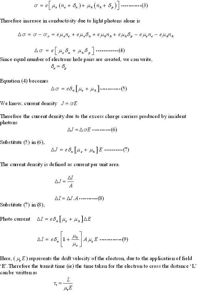
    Now when the light is allowed to fall on the detector, electron hole pairs are generated equally. These excess carriers increase the conductivity. If  and  are the excess carrier densities of electrons and holes respectively, then the electrical conductivity due to addition of these charge carriers is


THERMOGRAPHY :


    It deals with the measurement of heat emitted from a source without having contact with the source. The device that measures the temperature along with the images of the source which is emitting the heat is called thermal imaging camera.


Thermograms (or) IR imaging systems:


  •     Spot radiometer (or) point radiometer.
  •     2D thermograph (IR camera).

2D-THERMOGRAPH :


Principle:


The IR radiations from the object are detected and are converted into shades of gray. There shades of gray represent the temperature levels of the surface of the object over CRT screen.


Construction:

The IR camera consists of a plane mirror which is oscillating about a horizontal axis and an eight sided prism. Both can be rotated using motors.


The detector system is made of Indium antimonide which converts heat radiation into electrical signal. A separate cooling arrangement is made to cool the detector by placing liquid N2 into a dewar flask.

Working:

The IR radiation from the object is focused onto the oscillating plane mirror. This provides the vertical scanning of the object and the synchronized signal can be sent to display unit.(signal 1).

The image from the oscillating mirror is focused onto a rotating eight sided prism. This provides the horizontal scanning and the synchronized signals (signals 2) are sent to display unit.

These two signals (signal 1 and signal 2) produces an image of the object in the CRT display unit. The radiation from the eight sided prism is allowed to fall on the detector, after passing through the lens system.

Now the detector converts the IR radiation into electrical signals and is fed to the display unit after suitable amplification. The electrical signals produced depends on the energy of the incident radiation over the detector. Thus the signals modulate the beams intensity in the CRT display.

Thus the shades of gray of various intensity level is displayed in CRT. Each portion of gray (black and white) represents the various temperature of the object.

A digital display unit can be fixed below the CRT so that the temperature corresponding to any particular point of the object can be viewed directly.


Advantages:

1.  It can be used to measure the temperature differences between any points of the object even upto 0.1oC.

2. Using colour display units we can find the temperature, with respect to the colours obtained on CRT.

Dome-shaped LED:


In the planar LED, The reflection loss is more because most of the emitted light strikes the material interface at an angle greater than the critical angle. Therefore they are totally internally reflected and will not come out of the interface, thus the light is lost. This loss of light due to internal reflection can be minimized by two ways.


    By making the ‘p’ material in the shape of a hemispherical dome. the angle at which the light strikes the interface can be made less than the critical angle and hence he light will not be lost by the total internal reflection.


    By covering he p-n junction by a plastic medium of higher refractive index in the shape of hemispherical dome, total internal reflection can be reduced. This LED is used for commercial purpose. Hence, usually the dome shaped hemispherical LED is preferred than planar LED’s.


Advantages:

    They are smaller in size.

    Its cost is very low.

    It has long life time.

    LED’s are available in different colours at low cost.

    It operates even at very low voltage.

    Response time of LED is very fast in the order of  secs.

    Its intensity can be controlled easily.

    It can be operated at a wide range of temperature .

PLANER LED:


Since the light is emitted from a plane surface it is called planar LED (or) surface emitting LED.

Principle:


    Injection luminescence is the principle used in LED’s. when LED is forward biased, the majority charge carriers moves from p to n and similarly from n to p region and becomes excess minority charge carriers. Then these excess minority charge carriers diffuse through the junction and recombines with the majority carriers in n and p region respectively to produce light.

Construction:


In order to increase the probability of radiative recombination, the thickness of the ‘n’ layer is taken higher than that of the thickness of the ‘p’ layer. Contacts are made with the help of Al in such a way that top layer of the ‘p’ material is left uncovered, for the emission of light. Biasing can be applied at the contacts. The whole p-n junction is surrounded by plastic material so that the losses due to reflection can be minimized.

Working:

    Due to forward bias, the majority carriers from ‘n’ and ‘p’ regions cross the junction and become minority carriers in the other junction (ie) electrons, which are majority carriers in ‘n’ region cross the junction and go to ‘p’ region.

    Similarly holes which are majority carriers in ‘p’ region cross the junction and becomes minority carriers in ‘n’ region,


By similar process, the excess of minority carriers are injected in both ‘p’ and ‘n’ regions. This phenomenon is called minority carriers injection. The electrons which are excess minority carriers in p-region recombines with the holes which are majority carriers in ’p’ region and emit light. Similarly, the holes which are excess minority carriers in ‘n’ region recombine with the electrons which are majority carriers in ‘n’ region and emit light.

    Therefore electron-hole pair recombination process occurs more and thereby producing light through the top layer of the p-material which is left uncovered.

Disadvantage:

    Reflection losses will be more.

Light Emitting Diode:


An LED is a semiconductor p-n junction diode which converts electrical energy to light energy under forward biasing. It emits light in both visible and IR region.

Theory:

    It is known that only the direct band gap semiconductors emit light in the p-n junction. We know the forbidden band gap energy is given by.


Therefore, the wavelength of the light emitted purely depends on the band gap energy express in electron volts.

Types of LED’s:

    There are two types of LED’s

    Planer LED.

    Dome shaped LED.


Different phosphors used in CRO screens:

 Phosphors:


    The luminescent crystal which exhibits phosphorescence are called phosphors. There are different kinds of luminescent crystals which exhibit the phosphorescence.

  •     Zns and CdS activated with Cu, Mn, Ag, Au etc.,

  •     Alkali halides activated with thalium.

  •     Compounds with luminescence in the pure form such as gadolinium sulphate, manganous halides, molybdates etc.,
  •     Oxide phosphors such as self activated ZnO and  activated with transition metals.
  •     Silicate phosphors such as Zinc ortho silicate activated with divalent manganese.
  •     Organic crystals such as anthrascence activated with naphthalene.

Among these various phosphors, the phosphors used for CRO screens are

  •     Zinc-ortho silicate for green will be used in CRO tubes for general purpose.
  •     Calcium-tungstate for blue will be used in CRO tubes for fast photography.
  •     Zinc-cadmium sulphate for white will be used TV receiver tubes.
  •     Zinc-sulphate activated with Ag is used in colour television for Blue colour.
  •     Zinc-cadmium sulphide activated with copper is used in colour television for green colour.
  •     Yttrium oxysulphide activated with Europium and terbium is used in colour televisions for red colour.


Applications of phosphors:

  •     Fluorescent.
  •     Cathode ray oscilloscope.
  •     Television
  •     Radar
  •     Nuclear and radiation detectors
  •     Scintillation counters.

Phosphorescence:


The energy levels for the activators and co-activators are respectively known as hole and electron traps, which are similar to the acceptor and donor energy levels lie in the energy gap in between the conduction and valence bands.

    The absorption energy of the solid creates an electron-hole pair. Then the holes are quickly trapped holes leads to luminescent emission. It is also possible that the trapping of electrons occur at the donar site before recombination and trapping of a hole by the acceptor level. The electron may recombine with a trapped hole and hence release a luminescent radiation. The time taken by the electron in a trap depends on the depth of the trap and temperature.


    In this material, the emission of light occurs rather slowly due to the electron- hole recombination which takes place indirectly through the impurity levels. Therefore this process is known phosphorescence or slow photo luminescence.


Dielectric loss:


 It can be shown that the imaginary part of the dielectric constant  is a measure of the absorption of energy by the dielectric from the alternating field. The electric current density in the material due to the external alternating field.


This imaginary part of the dielectric constant  is related to the component of the current which is in phase with the applied field. This component of the current gives rise to absorption not the other component which is900 out of phase with the field. The energy absorbed by the dielectric per m3 per second is given by


Hall Effect


The conductivity measurements are not sufficient for the determination of the number of conducting charge and their mobility. Moreover these measurements do not give any information about the sign of the prominent charge carrier. The Hall Effect supplies the information of the sign of charge carrier.


When a magnetic field is applied perpendicular to a conductor carrying current, a voltage is developed across the specimen in the direction perpendicular to both the current and magnetic field. This phenomenon is known as Hall Effect.

Consider that an external electric field is applied along the axis of specimen, and then the electrons will drift in opposite direction. When a magnetic field is applied perpendicular to the axis of the specimen, the electrons will tend to be deflected to one side. Of course, the electrons will not drift into space but a surface charge is developed. The surface charge then gives rise to a transverse electric field which causes a compensating drift such that the carriers remain in the specimen. This effect is known as Hall Effect.

The Hall Effect is thus observed when a magnetic field is applied at right angle to a conductor carrying a current.

Consider a slab of material subjected to an external electric field Ex along the x-direction and a magnetic field Hz along the z-direction as shown in Fig. 13. Due to the electric field a current density Ix will flow in the direction of Ex. Let us consider the case in which the current is carried by electrons of charge -e. Under the influence of the magnetic field, the electron will be subjected to a Lorentz force such that the upper surface collects a positive charge while the lower surface a negative charge.

Fig. 13 The geometry of the electric and magnetic field for a simple Hall effect calculation.


The accumulation of charge on the surface of the specimen continues until the force on moving charges due to the electric field associated with it is large enough to cancel the force exerted by the magnetic field.

Ultimately a stationary state is reached when the current along y-axis vanishes, a field Ey is set up. If the charges carriers are holes then the case will be reversed, i.e., the upper surface would become negative while the lower surface as positive. Thus by measuring the Hall voltage in y - direction, the information about the sign of charges may be obtained. In this way, the measurement of Hall voltage gives the information about the charge carriers.


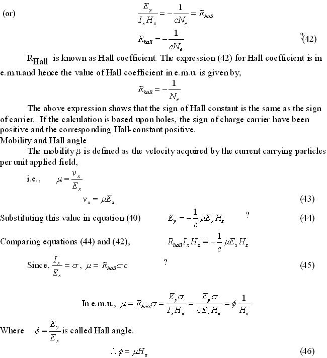
Hall voltage and Hall Co-efficient


Importance of Hall Effect


The measurement of the Hall Effect given the following important quantities:


1. The sign of the current carrying charges is determined.

2. From the magnitude of Hall coefficient the number of charge carriers per unit volume can be calculated.

3. The mobility is measured directly.

4. It can be used to decide whether a material is metal, semi conductor or insulator.


Here we should remember that not all the metals have negative Hall constant but some metals have a positive hall constant. (i.e., charge carriers are holes) and if both holes and electrons contribute to conductivity then RHall can be positive or negative depending upon the relative densities and mobilities of the carriers.

Antiferromagnetic materials and their properties:


1. This refers to spin alignment in an antiparallel manner in neighbouring magnetic ions resulting in zero net magnetization.


2. Magnitude of susceptibility is small and positive.

3. Temperature dependence of susceptibility: when
                                         

4. The opposite alignment of adjacent magnetic moments in a solid is produced by an (unfavourable) exchange interaction.

5. Initially susceptibility increases slightly as the temperature increases and beyond Neel temperature the susceptibility decreases with the temperature.

6. Neel temperature is the temperature at which susceptibility of the material is maximum.

7. spin alignment:


Eg:


FeO(ferrous oxide), MnO(Manganese Oxode), Cr2O3(chromium oxide) and salts of transition elements.

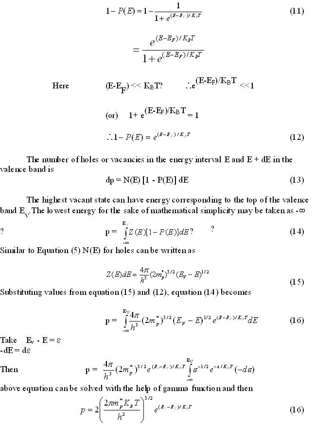
Carrier concentration in intrinsic semiconductors: Density of holes in valence band:


In an intrinsic semiconductor the number of electrons in the conduction band must be equal to the number of holes in the valence band. So the holes probability, that a state of energy E is unoccupied in the valence band, is


This equation gives the number of holes or vacancies in the valence band.


Superconducting Magnets & Magnetic Separator


A magnet consists of a superconducting coil in which current flow generating a large magnetic field. In the superconducting state the current flows without any resistive loss. So there is no Joule heating which is one of the major problems in the fabrication of high field conventional electromagnets. For example, to produce a field of 100 KG by a conventional magnet needs energy input of about 1MW.


The superconductors which are used for this application should have high critical fields. The most widely used materials are type II superconductor’s like Nb - Ti and Nb2Sn compounds. Low temperature superconductors are being used for fabricating superconducting Quantum interference devices (SQUIDs) which are used to measure magnetic fields and in medical diagnostics. A typical SQUID system for sensing magnetic field is shown in Fig 23.

A high speed levitating train (550 km/hr) making use of a conventional liquid helium superconductor material has been tested in Japan. Superconducting ship propulsion system with liquid helium superconductors also have been successfully tested in Japan.


Magnetic separator


Another application related to the production of magnetic fields is in magnetic separation. Ordinary electromagnets have long seen used for the processing of coal and other mineral raw materials to remove impurities. By passing the crushed solid material through a magnetic field, magnetic particles in the material can be diverted and collected Fig 24. With high strength magnetic fields, this technique can also be used in other process such as the removal of toxic metals from water, and the recovery of metallic catalysts from chemical rectors.


High Temperature SuperConductor (HTSC)


In early 1988, a new class of superconductor was discovered with unusually high TC values. Upto 1986, the highest TC value observed in the superconducting material is 23K. In 1986 superconducting cuprate discovered by Bednorz and Muller with TC value 30K, has the formula La2-xBaxCuO4. By 1987, materials discovered with TC value 93K and it rise to 125 K in 1988.The rapid increase in TC has led to the hope that it might be possible to develop materials that are superconductors at room temperature. Such materials could enable the transmission of electric power over long distances without resistive losses.


The high TC superconductors are oxides of copper in combination with other elements, They are ceramics, which means that they are brittle and hardly formed into wires to carry current. The crystal structure is characterized by planes of copper and oxygen between planes of the other element. The structure of orthorhombic YBa2CuO7 is given in Fig 22.

TYPES OF SUPER CONDUCTORS


Superconductors are classified into two types as type I and type II superconductors by magnetization behavior.


Type I superconductors

Type I superconductors behave as perfect diamagnetic materials and obey the Meissner effect. Fig 21 shows the relation between the magnetization produced and the applied magnetic field for type I superconductors.

 
 Fig 21 Variation of magnetization (M) with applied magnetic field (H)


A negative sign is introduced in the magnetization value to represent the diamagnetic property of the superconductor. The material produces a repulsive force up to critical field Hc. Therefore it does not allow the magnetic field to penetrate through it. Hence the material behaves as a superconductor. At Hc the repulsive force is zero; the materials behave as a normal conductor and allow the magnetic flux lines to pass through. They are soft superconductors used in coils for superconducting magnets.

Type II superconductors


Isotope effect


Meissner Effect


Meissner and Ochsenfeld (1933) found that if a superconductor is cooled in a magnetic field to below the transition temperature, then at the transition, the lines of induction B are pushed out Fig 19.


Followers